Flexibler Quarz-Oszillator auf Basis Si504
Published: Hardware Estimated reading time: ~4 minutes
A battery-friendly clock module as a building block for short wave tranceivers.
Why?
My first real transmitter 80m Selbstbau Transceiver mit Steuerung durch Arduino were centered around a Si570 as the oscillator and a class E power amplifier. Efficient operation was a major goal. While a class E power amplifier does give 80+% efficiency during transmit the same cannot be said for the oscillator portion. The Si570 covers an impressive frequency range: Even the least capable chip in the Si570 line can be operated between 3.5 ~ 210MHz. This unfortunately comes at the cost of high power consumption. The Si570 takes a fairly steady 90+mA at 3.3V. Another disadvantage is that the Si570’s officially guaranteed frequency range just starts at 10MHz. It works down to 3.5MHz but the chip then operates out of spec. Lower frequencies (160m band, LF, VLF) require external frequency divider circuits.
So I rejoiced in Silicon Labs’ announcement of a new oscillator in their pipeline which offeres the Si570’s frequency agility but at much reduced power consumption. On top of this it’s frequency range of 32kHz to 100MHz is a better match for the lower shortwave bands: Meet the Si540.
What followed was a rather long period of waiting until I finally found the chip in stock and ordered two.
Goals
Link to a discussion on qrpforum.de
- a tiny shielded module on a two-sided PCB, I am targetting a RF tight tinplate enclosure 37mm x 37mm x 20mm
- low power consumption: 50mW or less
- external power supply at 5V - 20V
- on-module low-noise regulated 3.3V power supply
- module pins excl. GND and VDD operate between GND and 3.3V and are not 5V tolerant
- frequency adjustments etc. over I2C
Prototype
The first prototype is built on a 100x160mm single-sided PCB using my strip-line approach. The Si504 got it’s own low noise power supply which is fed from a 12V battery. The battery compartment is screwed to the underside of the PCB. This is all mounted inside an Aluminum enclosure. The front cover has a power switch and a 9 pin Sub-D male socket. Eventually I can then talk to all the components inside this box over a serial interface. The back side of the box has a standard BNC female socket which routes the signal out of the box. Currently there is no microcontroller inside. My first experiments were done using an Arduino clone with an ATMega328P. I put that sketch into my Bitbucket repository.
The schematics is pretty simple:
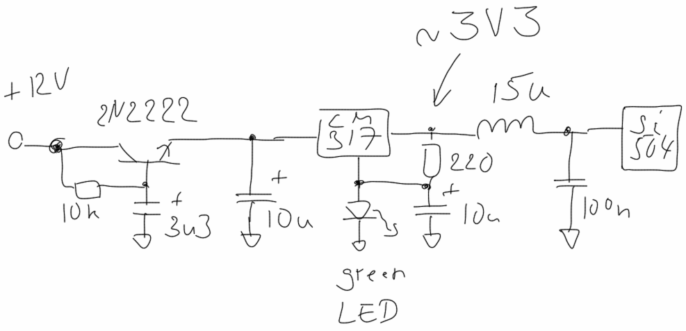
Abb. 1 - Si504 Powersupply
Left of the LM317 is a gyrator to filter out low frequence noise and present the LM317 with a realtively clean DC voltage. At it’s output terminal the LM317 has approximately 3.3V DC. By using a capacitor-bypassed LED as the second component to set the output voltage we get another reduction in AF to low RF noise. The 15uH/100nF low pass decouples RF coming from the Si504 from the DC rail.
Here are a few snapshots of the prototype:
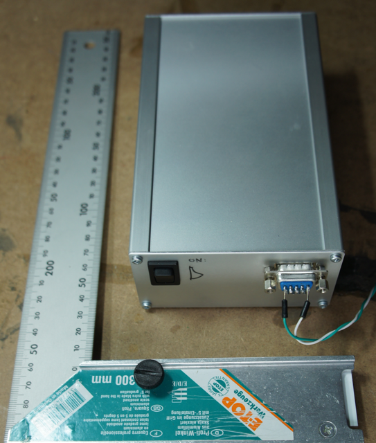
Abb. 2 - Enclosure
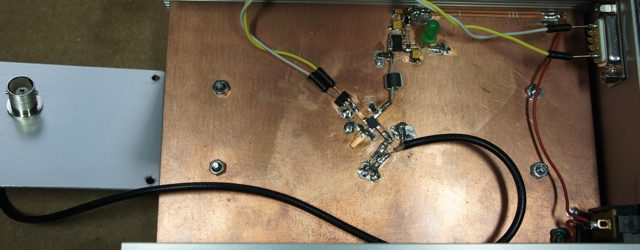
Abb. 3 - Inside the top view
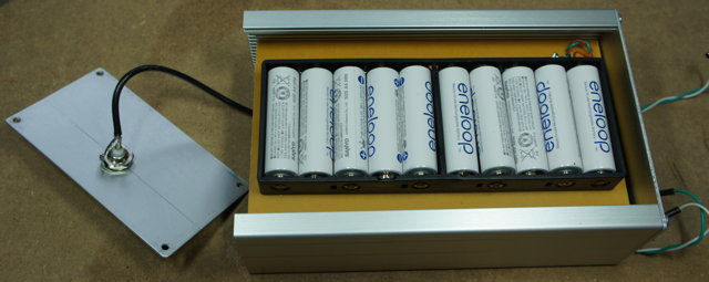
Abb. 4 - Inside bottom view
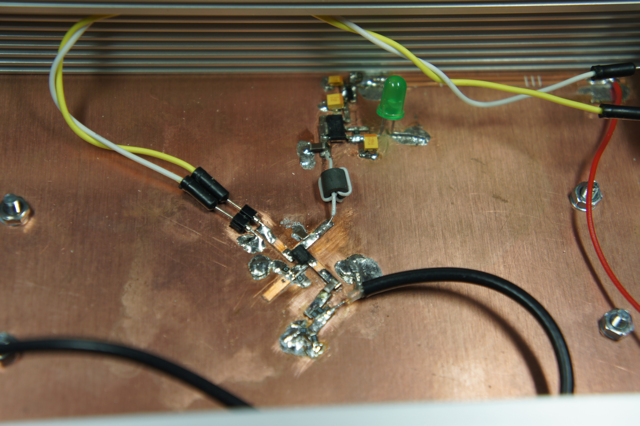
Abb. 5 - Details
Oscillator Performance
References for Phase Noise:
- Clifton Labs on Si570, AD9851, … Phase Noise Measurements
- More Information from Clifton Labs
- Hans Summers’ Estimation of Si570’ Phase Noise
- Si570 Phase Noise Plots
- Use the ELAD FDM-S1 for Oscillator Measurements
- Possible Buffers for Si504
- Audio Spectrum Analysis with Spectrum Lab
- Phase Noise Measurements with a Spectrum Analyzer
Setup for Phase Noise Measurements:
Output is approx. -10dBm into 50Ohm Spectrum Analyzer.
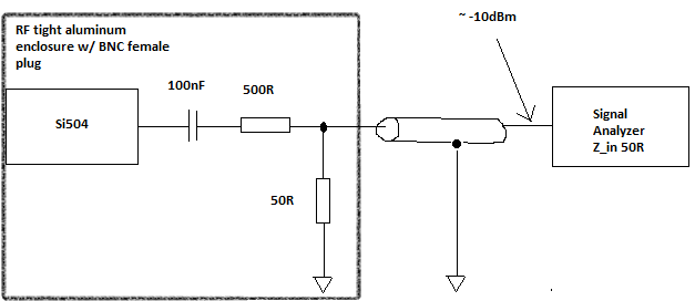
Abb. 6 - Setup
Phase Noise Measurements 1 (HP 8561B Spectrum Analyzer)
10kHz span, RBW 100Hz, VBW 10Hz.
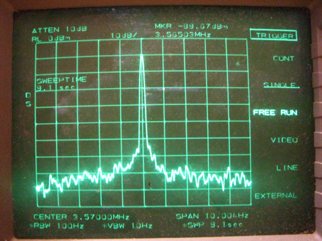
Abb. 7 - 3.57 MHz
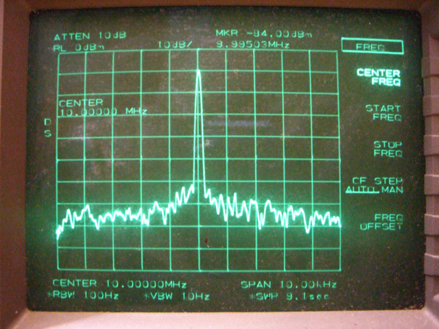
Abb. 8 - 10 MHz
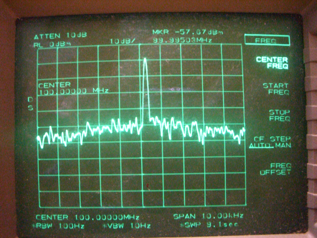
Abb. 9 - 100 MHz
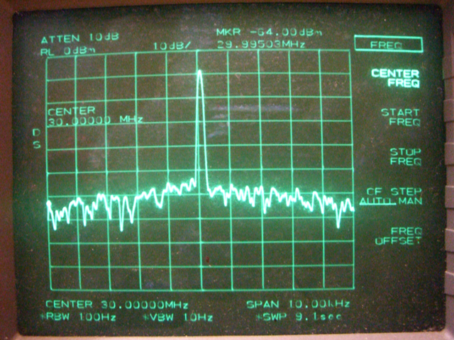
Abb. 10 - 30 MHz
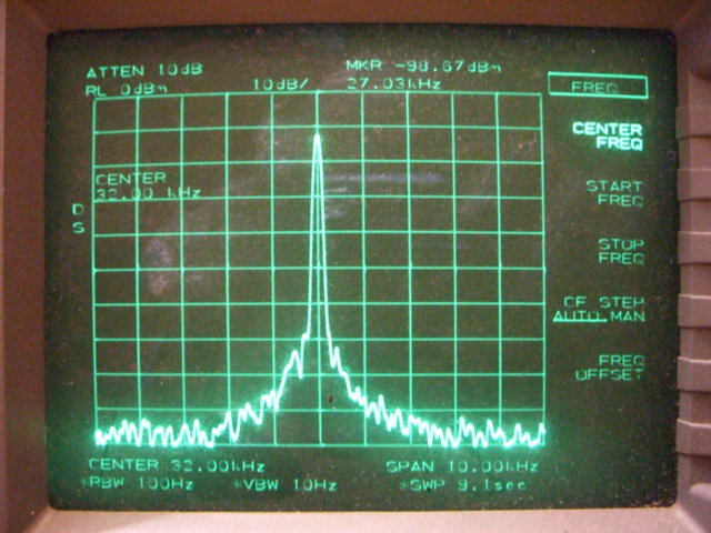
Abb. 11 - 32 kHz
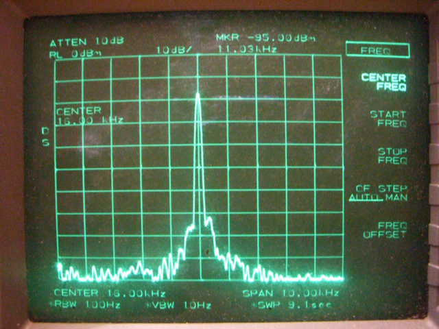
Abb. 12 - 16 kHz
As a comparison here you can see the spectrum of an HP 8654A Signal Generator set to 10MHz @ 0dBm output. The spectrum was recorded with the same RBW + VBW settings as the tests before.
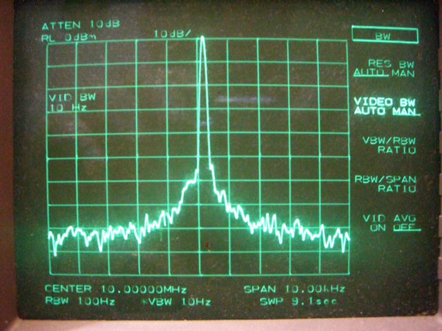
Abb. 13 -
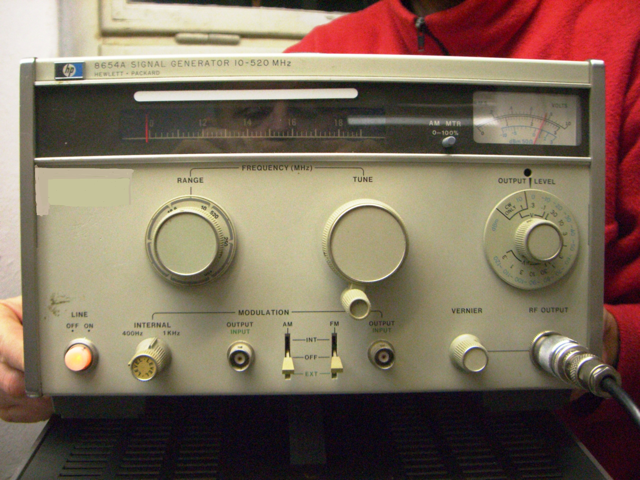
Abb. 14 - Here is a picture of the signal generator.
Phase Noise Measurements 2 (Rohde & Schwarz FSW)
Here are some results which were obtained with a Rohde & Schwarz FSW.
Unfortunately the first two measurements were done starting with an offset of 1kHz from carrier while all other start at 100Hz. Please also take note that the noise values are relative to the carrier (dBc) and the carrier here was approx. -10dBm.
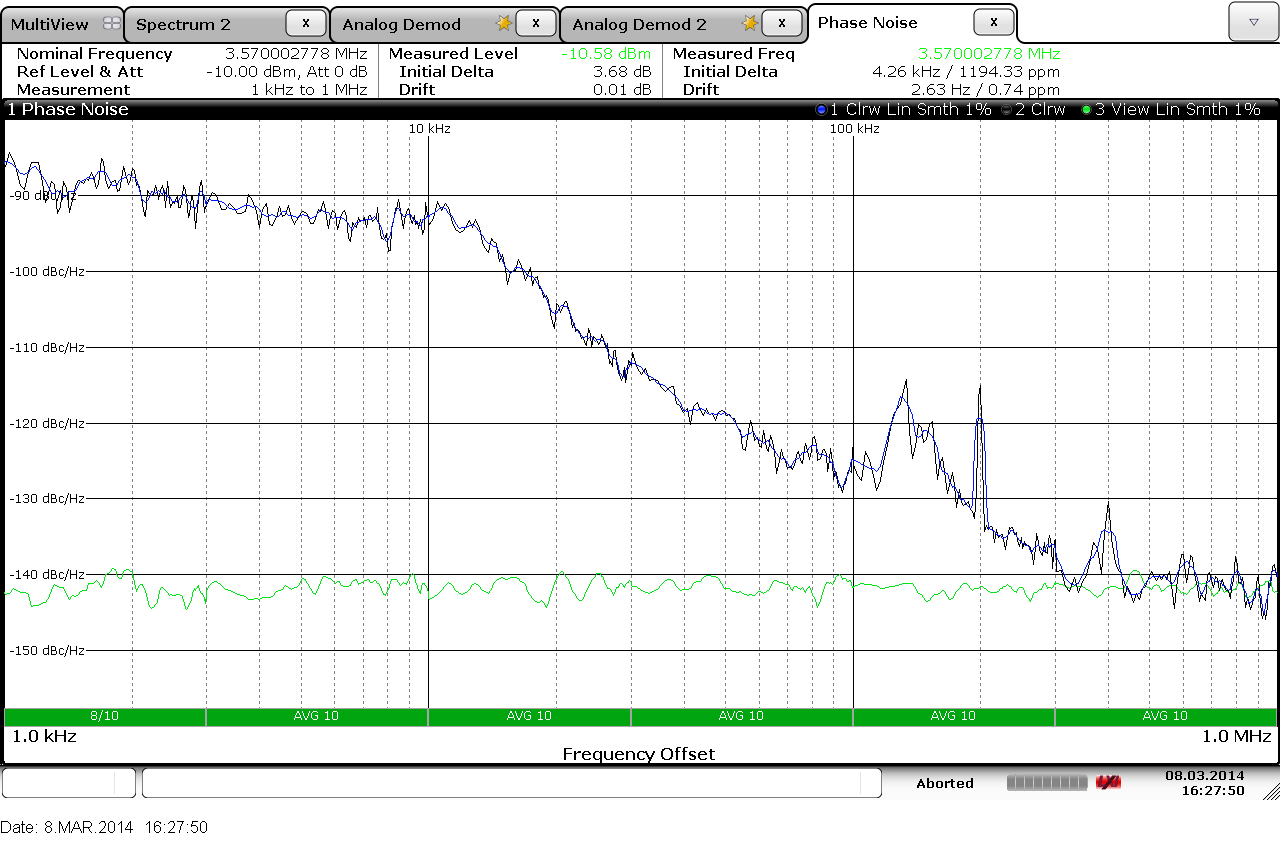
Abb. 15 -
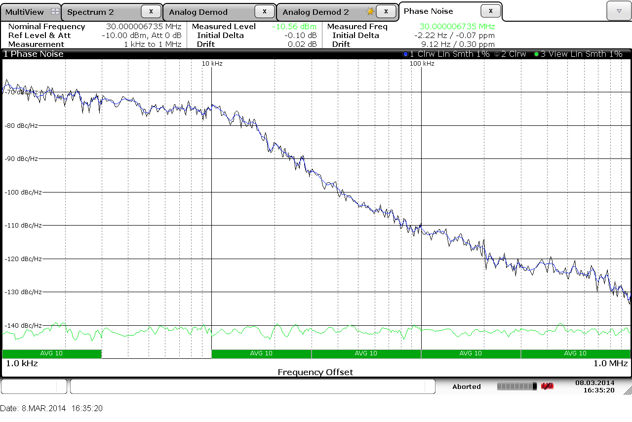
Abb. 16 -
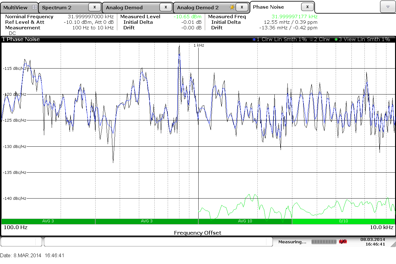
Abb. 17 -
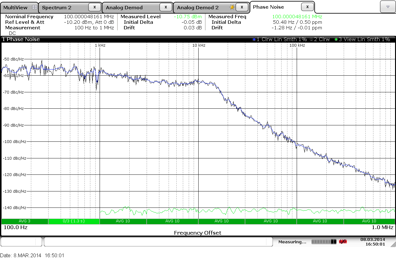
Abb. 18 -
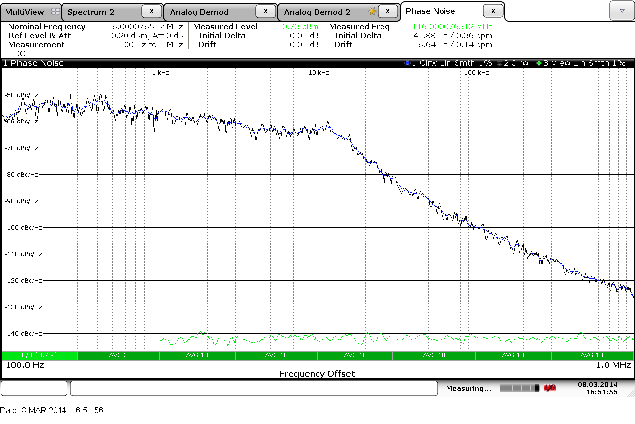
Abb. 19 -
Autor: Uwe, DO8UL